Lab 5
In lab_4 we drew the schematic of our board. Now let's do the layout of our PCB. We'll use the layout part of Eagle, along with perhaps the footprint editor and autorouter. This will conclude our exercises with PCB design; after this we'll move on to logic design with FPGAs.
Using the micboard.zip schematic (or your own schematic if you think is is better or more complete), turn your schematic into a daughterboard for the AVR32 bronze board. Please observe the following points:
- You will be doing a 2-layer daughterboard. Therefore your power must be routed in the signal layers. Pay attention that you try to keep the power routing to the digital and analog parts separate except where they join at the connections to a ground pin from the bronze board header.
- Keep sensitive electrical nodes far away from the noisy digital servo control.
- Place at least one bypass capacitor near the microphone preamplifier circuit.
- Don't put components over the AVR32.
- Check your board against this checklist of PCB design hints.
You may find it helpful to again scan the Eagle manual and tutoral (en de). You might also find it helpful to open the integrated help in Eagle, for instance while routing wires (ROUTE). The help shows you which mouse button and keys places vias, changes wire direction, changes layers, etc.
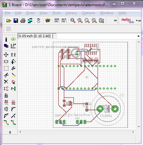
Below shows early progress on a partly finished board layout.
When you are finished with your board schematic and layout, send a zip/tgz archive of your design to tobi@ini.phys.ethz.ch?subject=micboard design for Electronics for Physicists II

