This is an old revision of the document!
Table of Contents
Lab 4
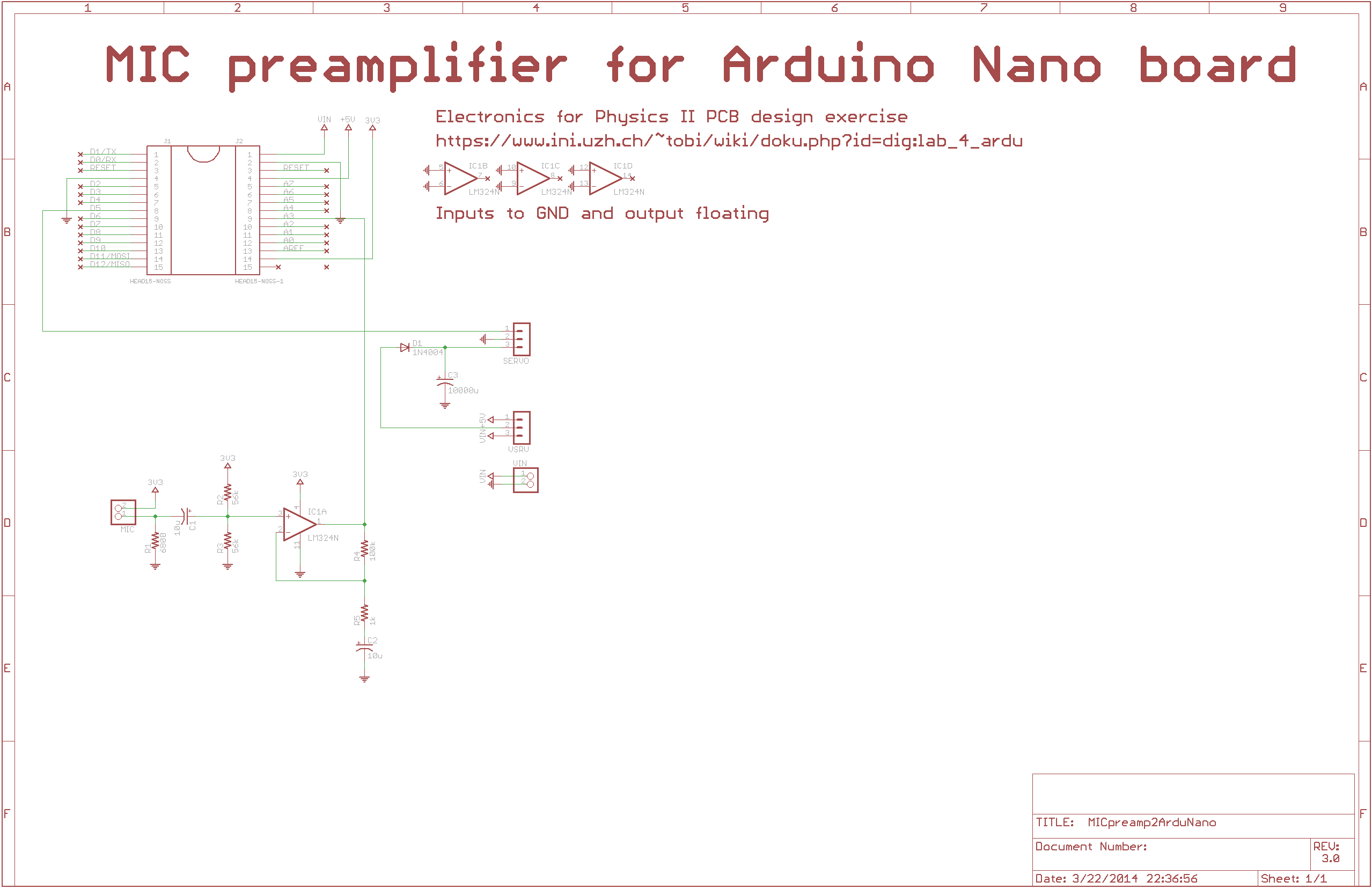
In lab_3 we built a prototype of our microphone-servo board. Now let's design the schematic of our own PCB. We'll draw a schematic of the microphone amplifier and servo supply and connector from lab 3, using the PCB design tool KiCad (formerly we used Eagle). It is not a very super powerful tool but installs very quickly, can run on multiple platforms, and has lots of user-developed parts libraries. We'll start today the layout of this board and you have time during next week to complete it and send by email.
This is an individual exercise and each student must complete it on their own laptop.
Preparation (before lab exercise)
- See pcb for the links to download the PCB design software.
Schematics Instructions
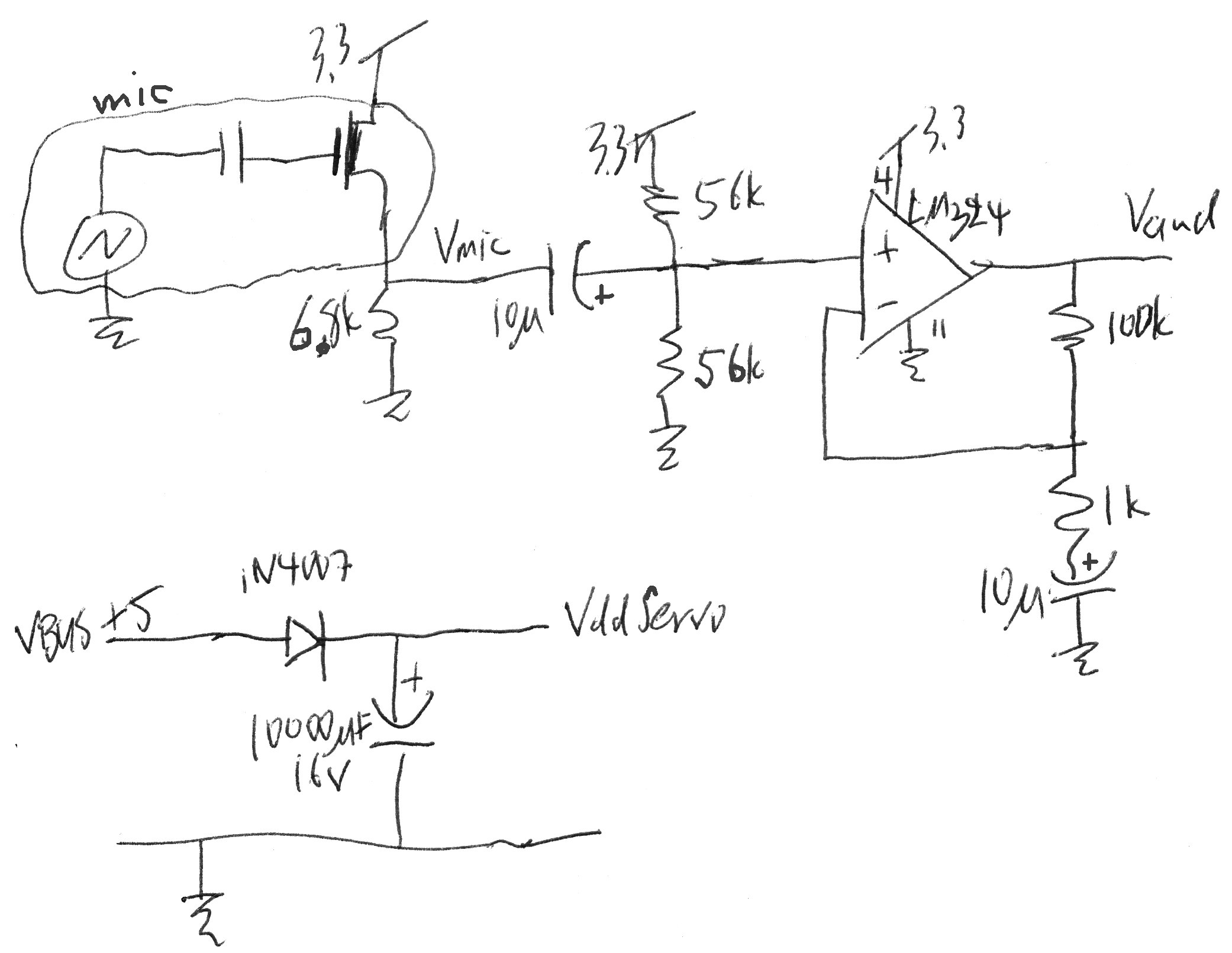
In this exercise we'll draw a schematic of the microphone amplifier and servo supply / connector from lab_3:
Remember that you actually modified some resistor values in lab_3 to bring the LM324 output more in the middle of it working range (see datasheet extract below).
- Install PCB software - see pcb.
- Launch the PCB software.
- Following the tutorial, make a new schematic and populate it with the needed components. You will need to download some libraries from pcb links and unzip/add these libraries.
- Wire up the parts according to the sketch above.
- Ensure your designators and values are correct.
- Place a large label indicating the design name and designer name (your name).
—-
When you are finished with your board schematic, zip your design and send it to tobi@ini.phys.ethz.ch?subject=micboard schematic for Electronics for Physicists II
LM324 tip
The LMC6484 is a rail to rail input and output opamp. However, the input range of the LM234 is limited:
Data sheets
- LM324 datasheet, SOIC-14 package, Library linear.lbr
- Power Diode datasheet, SMD, http://search.digikey.com/scripts/DkSearch/dksus.dll?Detail&name=641-1170-1-ND, Library DIODE-.lbr, footprint DIODE-20214AA
- Ultra capacitor, http://search.digikey.com/scripts/DkSearch/dksus.dll?Detail&name=P6975-ND. We might use an ultra-cap for the servo power supply bypassing but these are a bit tricky to select. You can find a large (>10k uF) aluminum capacitor instead if you like. Make sure your capacitor can handle >10V.
Layout Instructions
Now let's do the layout of our PCB. This will conclude our exercises with PCB design; after this we'll move on to logic design with FPGAs.
Please observe the following points:
- You will be doing a 2-layer daughterboard. Therefore your power must be routed in the signal layers. Pay attention that you try to keep the power routing to the digital and analog parts separate except where they join at the connections to a ground pin from the nano board header.
- Keep sensitive electrical nodes far away from the noisy digital servo control.
- Place at least one bypass capacitor near the microphone preamplifier circuit.
- Don't put components over the nano board.
You may find it helpful to again follow the tutorial.
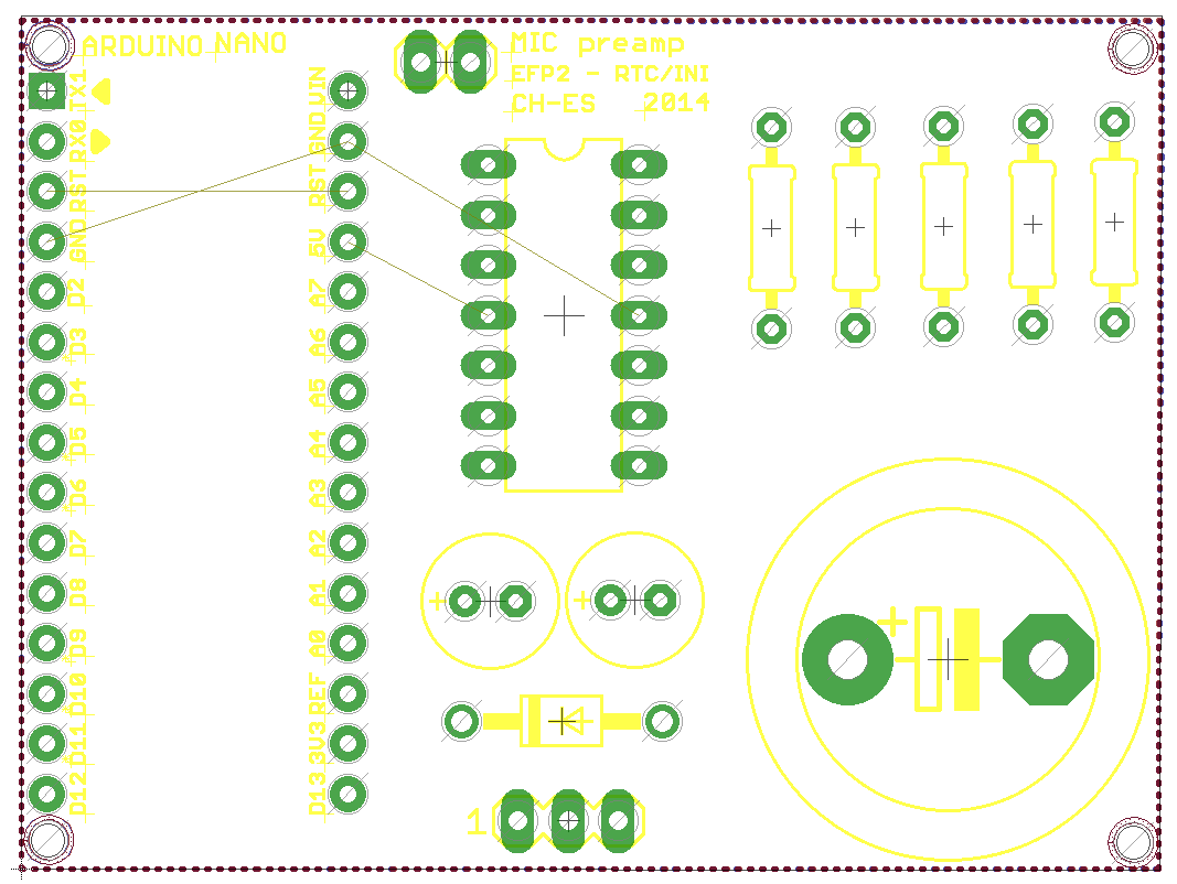
Below shows the template board layout.
When you are finished with your board schematic and layout, send a zip or tgz archive of your design to tobi@ini.phys.ethz.ch?subject=micboard design for Electronics for Physicists II
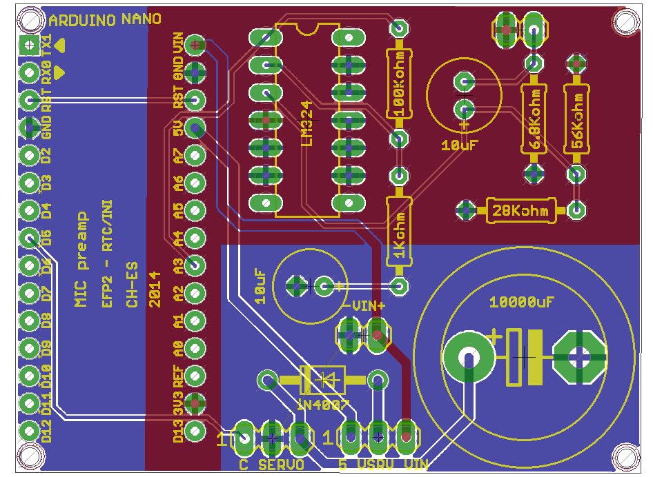
Here you have a screenshot of a possible solution (done using Eagle) that uses 2 layers. Polygons have been used for GND (bottom) and 3.3v (top).


